

AMD Vega 10 internal slides leak revealing GPU clock speeds


AMD Vega 10 internal slides leak revealing GPU clock speeds
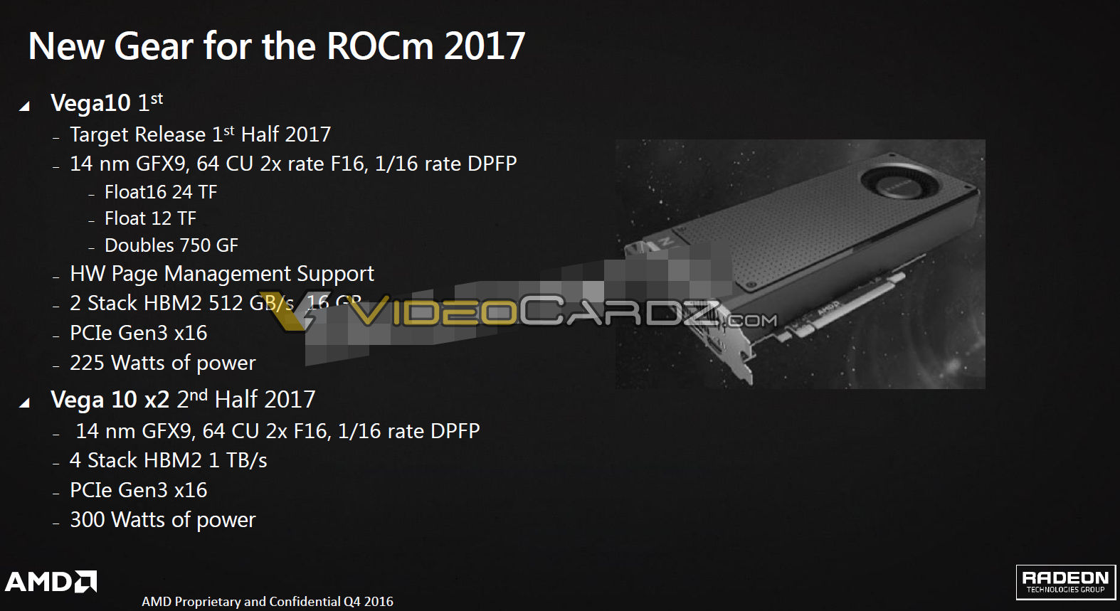
These slides reveal that Vega 10 will have 64 Compute Units (CUs) and offer at least 12TFLOPs of single precision compute performance. AMD has since then revealed their Vega powered MI25 GPU accelerator, which hints at increased compute performance of 12.5TFOPs, though this is in relation to professional grade GPUs, which are often clocked lower than their consumer counterparts.
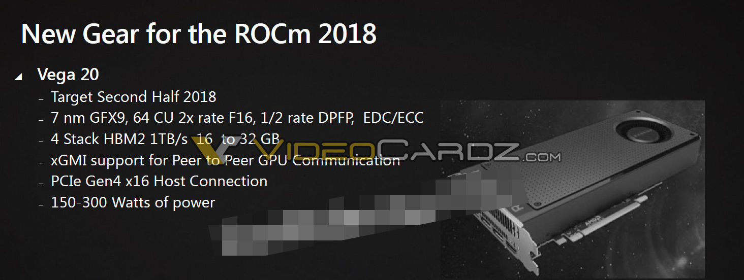
This slide also says that AMD’s Vega GPU will have a TDP of 225W, with a 300W dual Vega GPU planned for the second half of 2017. We can also see that this slide states that AMD’s Vega GPU will have two stacks of HBM2 memory, which matches the Vega GPU that was pictured at CES 2017.
To calculate the TFLOP performance of a GPU the following calculation is used.
FLOPs = Compute Units/Core Clusters x operations per clock (per CU) x GPU clock speeds
or
FLOPs = GPU Stream Processors x operations per clock (per core) x GPU clock speeds
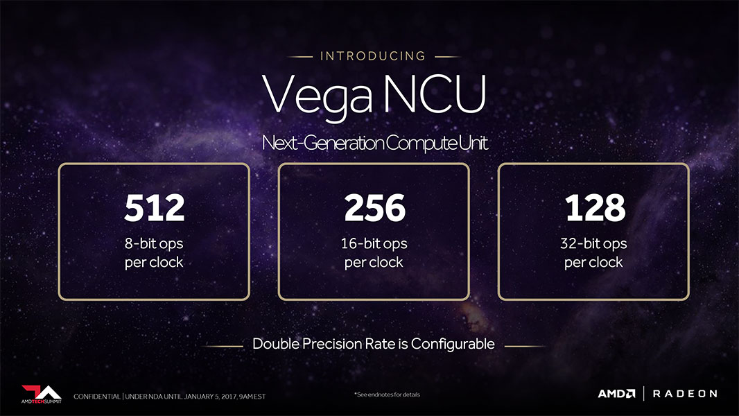
In these slides, we can see that AMD has 64 CUs in their Vega GPU architecture and in their recent Vega presentation they revealed that Vega Next Generation Compute Unit (NCU) offered 128 32-bit operations per second (see AMD slide below).
Traditionally AMD’s GCN based architectures have 64 Stream processors per CU and offered two instructions per clock for FP32 workloads, which delivers 128 operations per clock. This is the same number as AMD has used in their slide, hinting that AMD’s NCU is an upgraded design rather than a total redesign of their GCN CUs used in Polaris and Fiji.
With 64 Stream processors per CU and 64 total CUs AMD’s Vega GPU will have 4096 total stream processors. Using the equations above we can also calculate that for 12TFLOPs of performance AMD’s Vega GPU will need to be clocked at 1465MHz and for 12.5THFLOPs AMD’s Vega GPU will need to be clocked at 1525MHz.
From what we can see from these slides and some basic calculations AMD’s Vega GPU should have 4096 stream processors and clock speeds of around 1500MHz, though AMD may be able to improve the clock speeds of Vega before launch.
One thing that needs to be considered is that GPU performance is not just about TFLOP numbers, with AMD also making some significant changes to their memory architecture, geometry processing, their compute engine design and have implemented primitive shader and a new rasterization technique.
Looking at just AMD’s TFLOPs numbers does not tell the whole story with Vega, though a 50% increase in clock speeds over AMD’s Aging R9 Fury X is certainly a significant improvement. Hopefully, we will learn more about Vega’s gaming performance in the near future and exactly how AMD’s architectural improvements come into play.
You can read our full Vega GPU architecture analysis here.
You can join the discussion on AMD’s Vega 10 GPU clock speeds and design on the OC3D Forums.