


AMD Vega GPU architectural analysis

AMD Vega GPU architectural analysis
In both the compute world and the gaming world data sets have been becoming increasingly large, so much so that GPUs have simply not been able to keep up with the storage requirements of modern workloads.
GPU performance has been increasing at a much faster rate than memory (VRAM) capacity, with game installs becoming ever larger and texture requirements growing to insane levels. Today GPUs require a lot more VRAM than they did a few years ago, with 4GB becoming the norm for mid-range GPUs and 8GB starting to become commonplace.
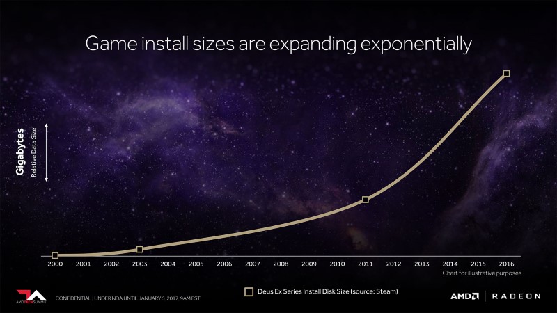

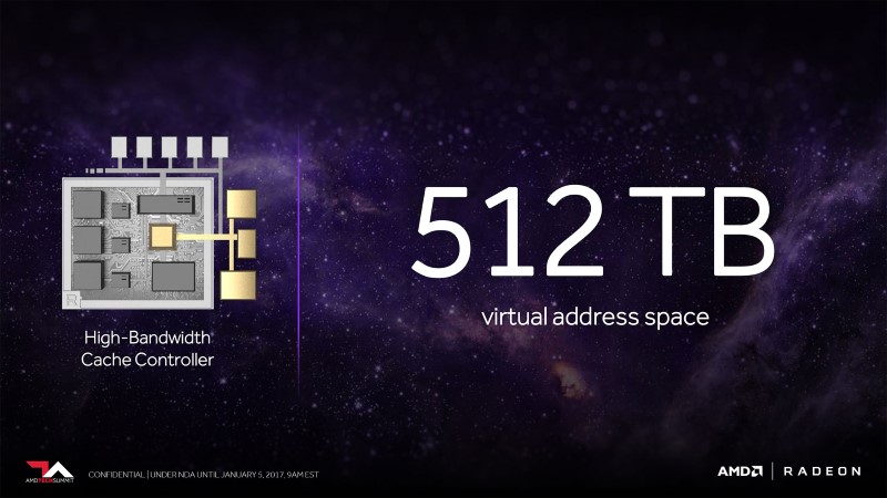
With resolutions reaching ever higher, compute loads getting more data intensive and game textures becoming increasingly large AMD thinks that a radical new memory solution is required for future GPUs, one that looks beyond traditional VRAM and into data sets that can reach up to 512TB in size.
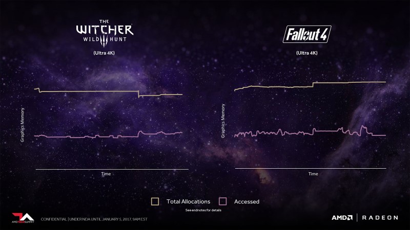
In modern gaming workloads, VRAM requirements can reach insane levels, though AMD has noticed an interesting trend, where games can require in excess of 8GB of VRAM but only require access to around 50% of the allocated data under most situations.
With only 50% of this data being used for a meaningful amount of time, it is reasonable to think that there can be a better way to manage video memory, perhaps one where not all of this data needs to be on your GPU’s VRAM.
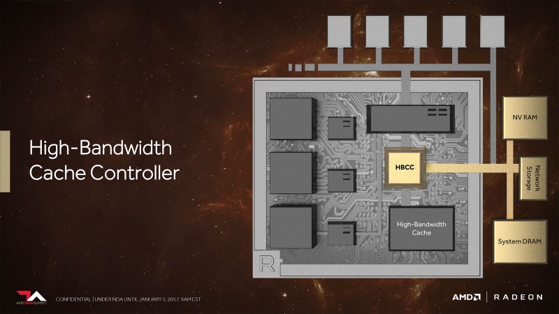
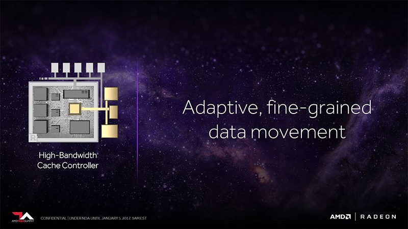
AMD’s solution to memory capacity problems is radical creating a new High Bandwidth Memory Controller (HBC) which allows the GPU to access memory outside the GPU alongside the GPUs traditional VRAM storage.
AMD is very vague about this new memory technology, but it effectively allows their Vega GPU to use data from your system memory, NVRAM (Non-Volatile flash storage) and even Network storage solutions. In effect this allows AMD’s Vega GPU to address up to 512TB of storage alongside the GPU’s HBM2 memory, allowing the GPU to use a seemingly limitless pool of storage if managed correctly.
AMD has showcased this type of memory solution before with their Radeon Pro SSG (Solid State GPU), which used an onboard M.2 NVMe SSD to have a frame buffer of 1TB. This solution was a clunky solution though it certainly leads to what we see now.
With Vega AMD is renaming what we would traditionally call a Frame Buffer (or VRM) into High Bandwidth Cache, which means that Vega’s HBM2 memory sits at the top of this while new GPU memory hierarchy and acts just as before, though now it completely changes what happens when the GPU “runs out of onboard memory”.
With normal GPUs when your run out of VRAM while gaming performance tanks, though now through clever memory management that may not be the case, with AMD’s new controller cleverly placing certain pieces of data into suitable memory for minimal performance impact. If this solution is implemented correctly user may not even notice if AMD Vega uses more than its traditional frame buffer, which is set to be a, not insubstantial, 16GB.
In the past, if you needed to use more memory than was in your GPUs frame buffer you would need to use your system memory, which adds a lot of latency and can slow performance down to a crawl, though with AMD’s new solution data can be allocated in a clever way to increase available memory without such a huge performance impact.
Previous solutions for this problem simply are not clever, adding a lot of needless latency and allocating data in a way which is not well suited to how often that data needs to be accessed and how quickly that data needs to be accessed.
With AMD’s Radeon Pro SSG, which accessed additional onboard memory through windows and not directly like their new Vega GPU, the company work with and scrub 5K videos in real-time at 90 frames per second, whereas current GPU offerings using traditional memory overflow methods was only able to achieve a mere 17FPS.
To say this least this memory allocation and control technology is exceptionally interesting and gives AMD the opportunity to become performance leaders in the High-Performance Compute market.
This technology will also have a huge impact on gaming performance, though only in scenarios when your GPU uses more than its onboard VRAM, which will play a significant role in the long-term usability of future AMD GPUs as textures get larger and games require more and more GPU memory.
On the next page, we will be discussing the changes to AMD’s Vega GPU Geometry and Compute capabilities.