

Samsung Plans to Mass Produce 3nm GAAFET Chips in 2021

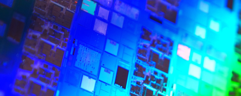
Samsung Plans to Mass Produce 3nm GAAFET Chips in 2021
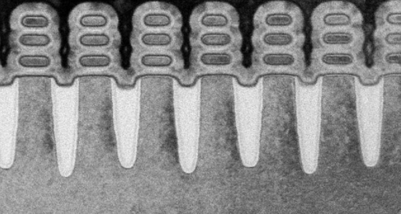
The name GAAFET describes everything that you need to know about the technology. It overcomes the scaling and performance limitations of FinFET by featuring four gates around all sides of a channel to offer full coverage. By comparison, FinFET effectively covers three sides of a fan-shaped channel. In effect, GAAFET takes the idea of a three-dimensional transistor to the next level.
Wrapping the gate around the channel reduced potential voltage losses, increasing transistor efficiency in the process. This allows lower supply voltages to be used, allowing for improved power efficiency.
Samsung has been developing their GAAFET technology for a number of years, with the company’s previous estimates placing the launch of 4nm GAAFET technology as early as 2020. Samsung is also expected to be the first company to launch a 7nm EUV process node, with plans to start production later this year. Their competitor, TSMC plans to implement EUV technology into their 7nm + node, a successor to their current-generation 7nm process.
If Samsung’s estimates are correct, the company has a shot at becoming the world’s leading silicon foundry within the next few years, though that does not mean that TSMC is out of the running. Nvidia is currently rumoured to be a launch partner for Samsung’s 7nm EUV process node.
You can join the discussion on Samsung’s 3nm GAAFET plans on the OC3D Forums.