


Samsung reveals 12-layer 3D-TSV chip breakthrough – Huge implications for HBM memory

Samsung reveals 12-layer 3D-TSV chip breakthrough – Huge implications for HBM memory
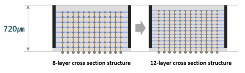
Using 60,000 TSV holes, Samsung can vertically stack 12 DRAM chips to create a three-dimensional structure, allowing the company to develop HBM memory chips that are up to 24GB in capacity. This feat is accomplished by stacking 12 16Gb chips. Amazingly, Samsung has been able to achieve this without any increase in size over today’s 8GB HBM2 memory packages.Â
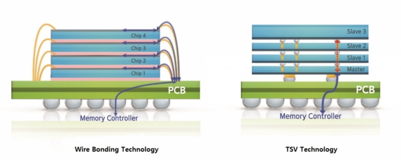
Thanks to the shorter data transmission time between chips, Samsung’s 12-layer 3D-TSV technology can also enable faster memory speeds and lower levels of power consumption than existing wire bonding technologies.Â
With this new technology, Samsung’s HBM2 memory could be used to create a Radeon VII-style graphics card with up to 96GB of HBM2 memory. Today, HBM2 memory is popular in a variety of use cases that extend from graphics cards to FPGAs and AI accelerators. Offering high capacity HBM memory modules will enable these products to work with larger data sets, which will in-turn help to push these technologies forward.Â
At this time, Samsung has not revealed a release timeframe for its 12-layer HBM products, though we expect to hear more in the coming quarters. Â
Â
 Â Â
    Â
 Â
You can join the discussion on Samsung’s 12-layer 3D-TSV technology on the OC3D Forums. Â