


NVIDIA Details Pascal GPU at GTC Japan


NVIDIA Details Pascal GPU at GTC Japan
Â
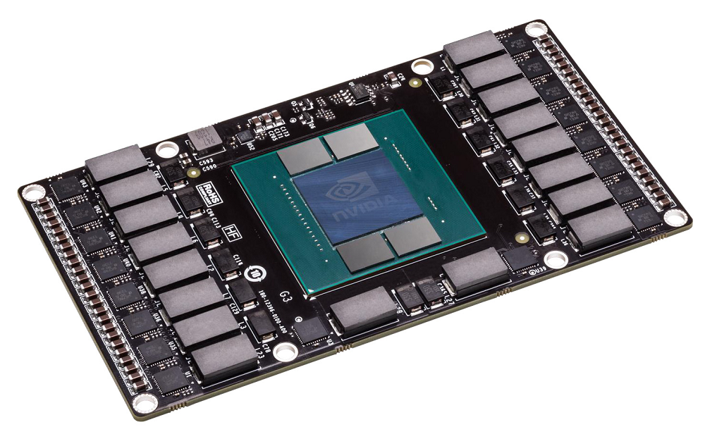
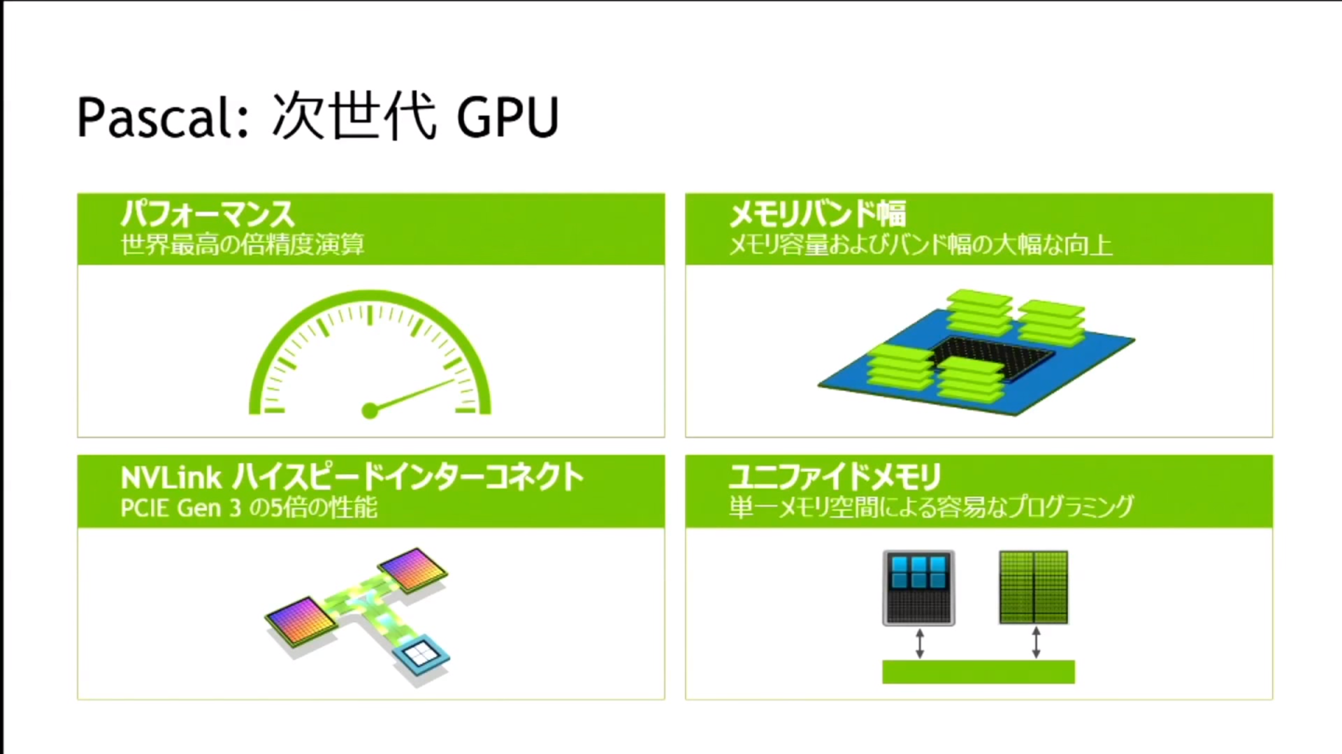
NVIDIA has detailed their Pascal GPU architecture at GTC Japan, saying that it will offer 2x the performance per watt of their already efficient Maxwell architecture and will contain a max of 16GB of HBM2 memory for consumer GPUs.Â
Nvidia’s Pascal GPUs will be built using TSMC’s 16nm process, which is not just a smaller processing node, but a process which uses FinFET transistors, which will offer a great performance leap over the 28nm planar transistors used in current generation GPUs.Â
    Â
 Â
The move to 3D memory from traditional planar GDDR5 memory will not only give a massive leap in GPU memory performance, but also allow increased capacities, with 4x4GB HBM2 memory giving consumer Maxwell GPUs up to 16GB of VRAM.Â
NVIDIA’s Marc Hamilton had this to say about HBM and Nvidia’s NVlink:
Â
“Using 3D memory, not only the memory capacity will go up, the memory bandwidth will go up significantly. With a much faster GPU, and higher memory bandwidth, the existing interconnects in the server are just plain outdated. So, we had to develop our own interconnect called NVLink, five times faster than existing technology.â€
Â
 Â Â
 Â
The next generation of GPUs from both AMD and Nvidia will be very interesting indeed, with both sides saying that they will get a 2x jump in performance per watt, moving to FinFET transistors and moving to use HBM 2.0 memory.Â
These next generation GPUs are expected to come in early to mid 2016.Â
Â
You can join the discussion on Nvidia’s Pascal GPUs on the OC3D Forums.Â
Â
Â
NVIDIA Details Pascal GPU at GTC Japan, offering 2x the performance per watt of Maxwell. https://t.co/raSryATjwh pic.twitter.com/B6kuMrKV9y
— OC3D (@OC3D) November 18, 2015