


AMD reveals their 7nm Vega Instinct MI60 and MI50 graphics cards

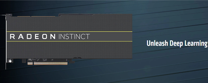
AMD reveals their 7nm Vega Instinct MI60 and MI50 graphics cards
For starters, AMD has worked to deliver the industry’s highest levels of FP64 compute on a single graphics card, reaching 7.4 TFLOPS on their MI60 graphics card, something that is unmatched within the industry, surpassing even Nvidia’s Turing-based Quadro RTX 8000. On top of that, AMD’s Radeon Instinct MI50 and MI60 graphics cards also offer support for PCIe 4.0, a first for the Datacenter GPU market.Â
Thanks to AMD’s use of TSMC’s 7nm process node, the company has been able to condense their Vega GPU design to a die size of 331mm squared, while also adding two additional memory controllers to support four HBM2 dies. This allows the Radeon Instinct 60 to support up to 32GB of HBM2 memory. Â
In terms of core clock speeds, 7nm Vega offers a significant boost over AMD’s 14nm design, boosting the graphic’s card’s peak clock speeds from 1500MHz in the MI25 to 1800MHz on the MI60, an increase of 20%. This showcases the performance benefits of TSMC’s 7nm process node, especially after considering the fact that the MI60 has the same 300W TDP as the MI25, while also requiring 8-pin + 6-pin power configuration.Â
AMD has made it clear that their 7nm Vega graphics cards are not designed for gaming applications, instead, acting as a way for the company to enter the lucrative server/datecenter and machine learning markets.Â
Â
|  | Radeon Instinct MI60 | Radeon Instinct MI50 | Radeon Instinct MI25 |
| Microarchitecture | Vega | Vega | Vega |
| Lithography | 7nm | 7nm | 14nm |
| Compute Units | 64 | 60 | 64 |
| Stream Processors | 4096 | 3840 | 4096 |
| Peak Engine Clock | 1800MHz | 1746MHz | 1500MHz |
| Peak FP64 TFLOPS | 7.4 TFLOPS | 6.7 TFLOPS | Â |
| Peak FP32 TFLOPS | 14.7TFLOPS | 13.4 TFLOPS | 12.29 TFLOPS |
| Peak FP16 TFLOPS | 29.5 TFLOPS | 26.8 TFLOPS | 24.6 TFLOPS |
| Peak INT8 TFLOPS | 58.9TFLOPS | 53.6 TFLOPS | Â |
| Memory Type | HBM2 | HBM2 | HBM2 |
| Memory Capacity | 32GB | 16GB | 16GB |
| Memory Interface | 4096-bit | 4096-bit | 2048-bit |
| Memory Clock Speed | 1,000MHz | 1,000MHz | 945MHz |
| Memory Bandwidth | 1,024 GB/s | 1,024 GB/s | 484 GB/s |
| ECC Support | Yes (Full Chip) | Yes (Full Chip) | Yes |
| TDP | 300W | 300W | 300W |
| PCIe Support | PCIe 4.0 | PCIe 4.0 | PCIe 3.0 |
| Power | 8-pin + 6-pin | 8-pin + 6-pin | 8-pin + 8-pin |
Â
When looking at AMD’s 7nm Vega graphics cards, it is clear that the company sees a future in AI compute, though at this time it is unknown whether or not the company plans to bring their AI performance into the gaming market, mirroring Nvidia’s moves with Turing. With the 20% clock speed gains through their use of 7nm technology, I’m excited to see what the company will be able to achieve when they eventually decide to bring 7nm to gamers, especially when combined with a next-generation graphics architecture like Navi.
Sadly AMD’s announcements today didn’t reveal any of AMD’s future graphics card roadmap, or hint at the release of any new Radeon graphics hardware for the consumer market.Â
You can join the discussion on AMD’s 7nm Vega Instinct MI60 and MI50 graphics cards on the OC3D Forums.Â