


Intel intros a new node naming scheme – 10nm Enhanced SuperFin is now Intel 7


Intel intros a new node naming scheme – 10nm Enhanced SuperFin is now Intel 7
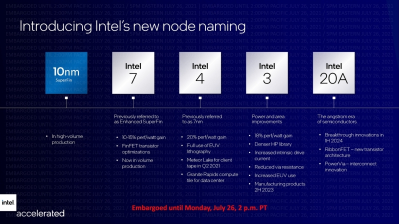
10nm Enhanced SuperFin Becomes Intel 7Â
Lithography Node names are traditionally linked with gate widths, but as process technology continued to get smaller and smaller, node names diverged from this key metric. New transistor designs and enhanced node characteristics allowed manufacturers to improve the performance and efficiency of their transistors without gate size decreases, making node names based on gate size irrelevant.Â
TSMC, Globalfoundries and Samsung have all moved away from traditional node naming methods, and now Intel is doing the same. Intel’s 10nm node is similar in size to TSMC’s 7nm node on a per-transistor basis, which is why Intel’s new 10nm Enhanced SuperFin node will be called Intel 7.Â
What makes Intel 7 special?Â
Intel’s 10nm Enhanced SuperFin/Intel 7 node is now in volume production, and with this node, Intel has promised a 10-15% improvement in performance per watt, which is great news for Intel upcoming Intel 7 products.Â
The Intel 7 name signals that this node delivers similar characteristics to 7nm nodes from Samsung and TSMC. Intel has started producing more 10nm wafers than 14nm wafers this quarter, signalling that their 10nm/Intel 7 based products have now entered mass production.Â
Intel 7 will be used to create Intel’s Alder Lake desktop/mobile processors and the company’s Sapphire Rapids Server processors. Products based on Intel’s Intel 7 node will be launched this quarter with Alder Lake.Â
 Â Â
 Â
The future of Intel – An Accelerated Lithography Roadmap
Intel’s planned 7nm node has now been renamed to Intel 7, promising users a 20% performance/watt gain and smaller transistors through the “full use” of EUV technology. Intel’s “Intel 4” node will be used to create their Granite Rapids compute tiles for datacenter CPUs and to create the company’s Meteor Lake compute tiles. Â
Intel 4 will be 2x as dense as Intel 7, offer customers a 4x reduction in design rules and support Intel’s next-generation Foveros and EMIB technologies. Intel’s “Intel 3” node will deliver further benefits, with Intel planning to create products using the node in the second half of 2023.Â
Intel 20A – A Next-Gen Node
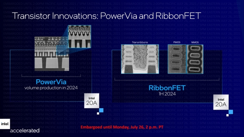
With Intel 20A, with A standing for Angstron (10^-10 m/0.1nm), Intel plans to offer their customers a fully next-generation process technology. Intel 20A will be a process node that’s based on GAAFET (Gate-All-Around FET) technology, utilising what Intel calls RibbonFET technology. RibbonFET will be Intel’s largest process technology shift since their move to FinFET in 2011.Â
Alongside RibbonFET, Intel will be utilising a new technology called PowerVia to enable backside power delivery, optimising signal transmission to improve the characteristics of their lithography process further. Moving forward, Intel also plans to create smaller process technologies like Intel 18A to enable further performance increases with refined RibbonFET transistors.Â
Alongside their new process technology roadmap, Intel has revealed enhancements to their packaging technologies to facilitate the creation of new 3D processors.Â
 Â
The critical thing to consider with these announcements is that they don’t exclusively apply to Intel’s own products. Though IDM 2.0, Intel will be opening up its fabs to 3rd parties to facilitate the creation of non-Intel products using Intel’s lithography and packaging technologies. Intel has confirmed that Amazon and Qualcomm will be Intel Foundry services customers, a change that will allow Intel to profit from its own products and those of its competitors. In theory, even AMD could manufacture their future processors at Intel’s fabs.Â
You can join the discussion on Intel new process technology naming scheme and technology roadmap on the OC3D Forums.Â
Â