


AMD Reveals Transformative “Chiplet” Design for Zen 2 EPYC Processors

AMD Reveals Transformative “Chiplet” Design for Zen 2 EPYC ProcessorsÂ
At their Next Horizon event, AMD confirmed that their Zen 2 based EPYC processors would utilise a revolutionary new “Chiplet” design model, splitting core aspects of the product into separate pieces of silicon, fulfilling AMD’s desire to have a fully modular CPU.Â
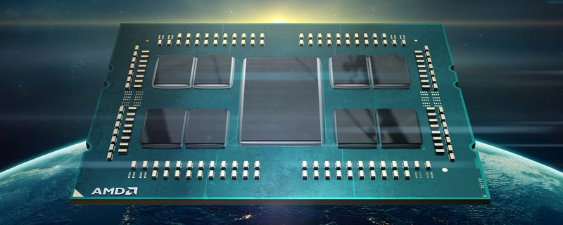
In the case of AMD’s 64-core Zen 2 EPYC CPUs, AMD is combining eight 7nm 8-core CPU modules with a larger 14nm module, solving many of the design shortcomings of today’s 1st Generation EPYC processors while delivering a design that promises to be relatively cheap to produce when compared to large monolithic (single-die) solutions.Â
Today’s EPYC (and Ryzen Threadripper) processors have their I/O split between several processors, with some PCIe lanes, DRAM channels etc attaching to specific dies on each processor, introducing some unwelcome latency when data from these lanes need to move from one processor to the other. With Zen 2 EPYC, AMD has centralised I/O operations into a single die, allowing all DRAM channels and PCIe data to reach applicable CPU cores with the same latency levels.Â
AMD’s modular design also allows the company to optimise their manufacturing processes for each section of an EPYC 2 processor. TSMC’s 7nm node offers the performance, power and density advantages that AMD needs to create a leading-edge processor core design while a 14nm (likely Globalfoundries) process is used to create AMD’s centralised I/O unit with a power-optimized chip that fulfils all of AMD’s requirements. I/O operations do not benefit that much from leading-edge process nodes, which is why AMD can afford to use 14nm instead of 7nm, lowering their manufacturing costs while delivering the functionality they require. Beyond that, 14nm will produce a larger chip that is more suitable for interfacing with EPYC’s large TR4-style package.Â
With such a large I/O die, it is also possible that AMD has added an extra layer of cache to their Zen 2 EPYC processors, a level 4 cache that will sit between the large processor and the system’s DRAM, though this has not been confirmed. Inside AMD’s large I/O die is support for eight DDR4 memory channels, 128 PCIe lanes (Zen 2 EPYC support PCIe 4.0) and interconnects/data paths for eight 8-core Zen 2 chips.  Â
 Â
 Â Â
 Â
This isn’t the first time that a modular processor of this type has been proposed, with Intel discussing multi-die processors back in 2017, utilising their high-speed, low-latency EMIB technology to merge several dies together to create a high-end processor. AMD has beaten Intel to the punch when it comes to creating multi-chip processor designs, taking a major step away from their original Zen/EPYC design to create a processor that is fully modular.Â
With Zen 2 EPYC in mind, we are left to wonder what the future holds for AMD’s desktop products, and even their semi-custom console chips. It is possible that we will see future consoles implement a similar multi-chip design, or see a variant of this design scheme on future Ryzen CPUs and APUs.Â
More information about AMD’s Zen 2 architecture is available here.Â
You can join the discussion on AMD’s “Chiplet” design for their Zen 2 EPYC processors on the OC3D Forums.Â