


Intel discusses EMIB technology – Multi-die CPUs incoming?

Intel discusses EMIB technology – Multi-die CPUs incoming?
 Â
 Â Â
 Â
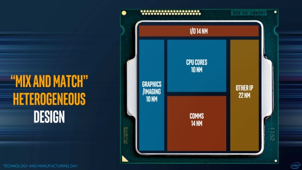
This plan goes beyond what AMD has done with Threadripper, with plans to create products with separate components that are all based on different process nodes. This allows Intel to have a more “Mix and Match” product design and it allows for each separate piece of a processor to be built using an optimised manufacturing process.Â
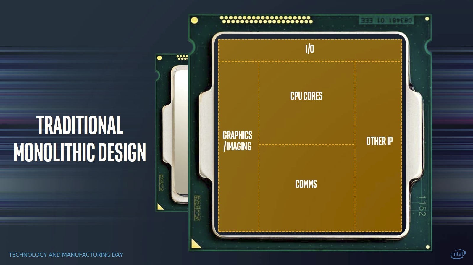
Intel plans to separate their CPUs into several smaller dies, allowing parts that don’t scale well to smaller process nodes to be built on older, mature process nodes while allowing certain aspects of a product to benefit from more advanced manufacturing techniques. This will allow the roll-out of new process nodes to happen faster and for legacy nodes to receive more use later in its life cycle.Â
The problems here arise when connecting these dies together, as the interconnect must be low power, low latency and high bandwidth to be effective.
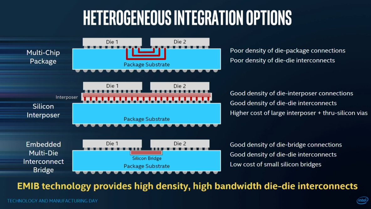
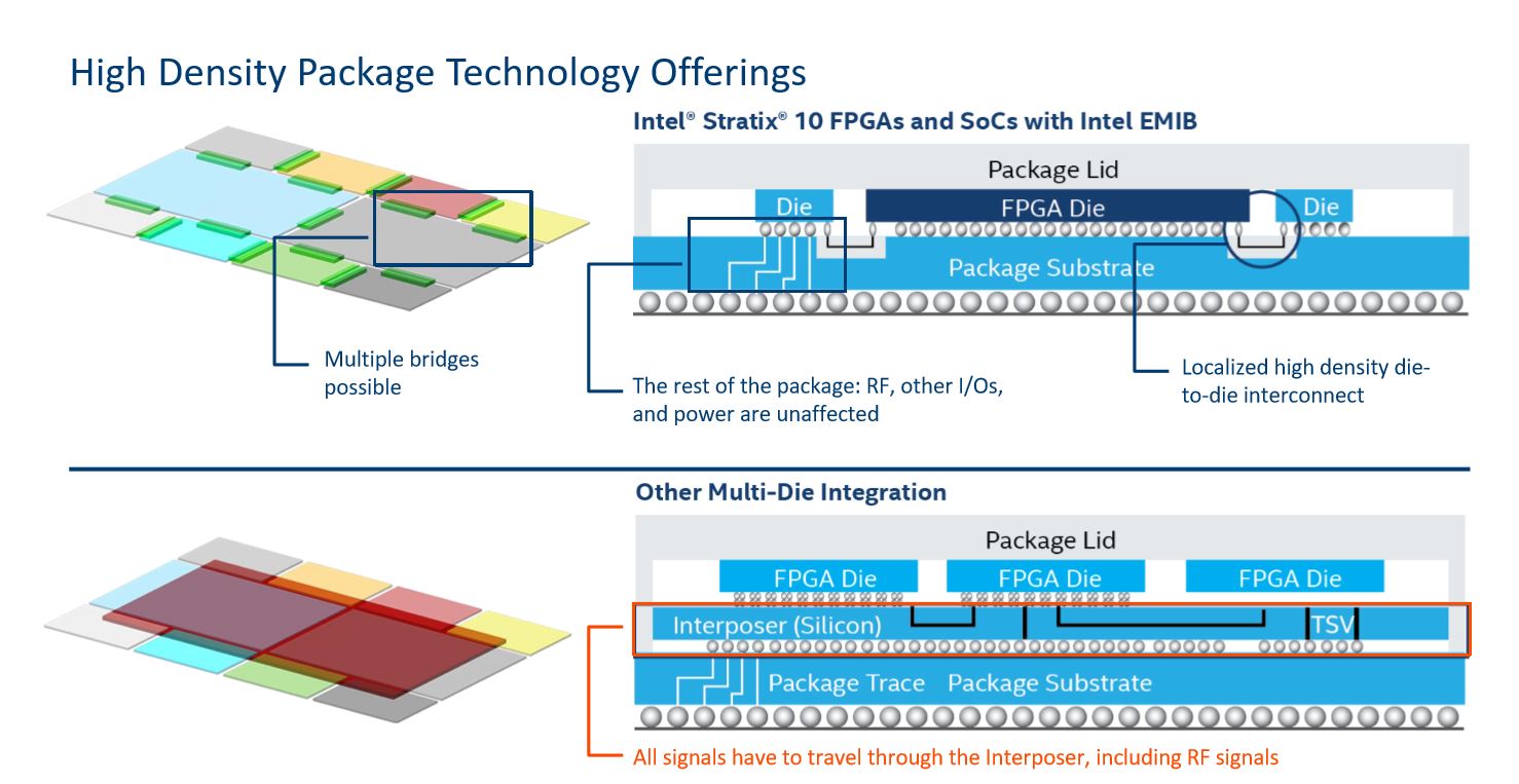
The main problem for multi-die connectivity is cost and density, with today’s solution typically being two options, using a Multi-chip package or a silicon interposer.Â
A multi-chip package is fairly simple, using the CPU package to connect each die, though the downside is that interconnects need to be spaced relatively far apart to function properly, limiting the number of interconnects that are possible.Â
Using an interposer between your silicon dies and package substrate has its own advantage, offering a fast interconnect with high levels of interconnect while also allowing the silicon to interact with the package underneath using TSV (Through Silicon Via) technology.
This solution is used by AMD to connect the HBM memory and GPU dies of their Fiji and Vega series GPUs. Sadly this solution is costly, with costs increasing further as the interposer gets larger, making it a bad solution for huge multi-die processors.Â
Â
Intel’s new solution is to use what they call EMIB (Embedded Multi-die Interconnect Bridge) technology, which solves some of the issues that are posed by the above solutions, using embedded silicon “bridges” into a package substrate to act as dense connectivity highways between multiple dies.  This gives silicon dies the ability to use die to package interconnects as normal, without going through an interposer, while offering more package-to-package interconnects when necessary. Â
This solution will cost less than using a full silicon interposer, in-theory, while offering the same connectivity benefits. This will be very important for Intel moving forward, especially as they design larger and larger multi-die CPU complexes. Â
Â
Intel sees the future not as producing singular chips for CPUs, but as the merger of several “chiplets”, allowing each piece of a product to be created using an ideal process while connecting to each other using a simple, affordable interconnects.Â
We are unlikely to see this technology in desktop components anytime soon, with this technology being best applies to Intel’s larger die products like Xeon CPUs. Intel could also use this tech to integrate XPoint memory onto future CPU packages, offering a large, fast Level 4 cache on future processors.Â
Â
You can join the discussion on Intel’s EMIB technology on the OC3D Forums.Â
Â
Intel discusses EMIB technology – Multi-die CPUs incoming?
 Â
 Â
 Â
This plan goes beyond what AMD has done with Threadripper, with plans to create products with separate components that are all based on different process nodes. This allows Intel to have a more “Mix and Match” product design and it allows for each separate piece of a processor to be built using an optimised manufacturing process.Â
Intel plans to separate their CPUs into several smaller dies, allowing parts that don’t scale well to smaller process nodes to be built on older, mature process nodes while allowing certain aspects of a product to benefit from more advanced manufacturing techniques. This will allow the roll-out of new process nodes to happen faster and for legacy nodes to receive more use later in its life cycle.Â
The problems here arise when connecting these dies together, as the interconnect must be low power, low latency and high bandwidth to be effective.
The main problem for multi-die connectivity is cost and density, with today’s solution typically being two options, using a Multi-chip package or a silicon interposer.Â
A multi-chip package is fairly simple, using the CPU package to connect each die, though the downside is that interconnects need to be spaced relatively far apart to function properly, limiting the number of interconnects that are possible.Â
Using an interposer between your silicon dies and package substrate has its own advantage, offering a fast interconnect with high levels of interconnect while also allowing the silicon to interact with the package underneath using TSV (Through Silicon Via) technology.
This solution is used by AMD to connect the HBM memory and GPU dies of their Fiji and Vega series GPUs. Sadly this solution is costly, with costs increasing further as the interposer gets larger, making it a bad solution for huge multi-die processors.Â
Â
Intel’s new solution is to use what they call EMIB (Embedded Multi-die Interconnect Bridge) technology, which solves some of the issues that are posed by the above solutions, using embedded silicon “bridges” into a package substrate to act as dense connectivity highways between multiple dies.  This gives silicon dies the ability to use die to package interconnects as normal, without going through an interposer, while offering more package-to-package interconnects when necessary. Â
This solution will cost less than using a full silicon interposer, in-theory, while offering the same connectivity benefits. This will be very important for Intel moving forward, especially as they design larger and larger multi-die CPU complexes. Â
 Â
Â
Intel sees the future not as producing singular chips for CPUs, but as the merger of several “chiplets”, allowing each piece of a product to be created using an ideal process while connecting to each other using a simple, affordable interconnects.Â
We are unlikely to see this technology in desktop components anytime soon, with this technology being best applies to Intel’s larger die products like Xeon CPUs. Intel could also use this tech to integrate XPoint memory onto future CPU packages, offering a large, fast Level 4 cache on future processors.Â
Â
You can join the discussion on Intel’s EMIB technology on the OC3D Forums.Â
Â