


AMD reveals a Exascale MEGA APU in a new academic paper

AMD reveals a Exascale MEGA APU in a new academic paper
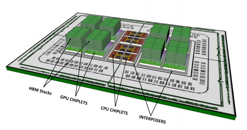
This new APU type will also use onboard memory, using a next-generation memory type that can be stacked directly onto a GPU die, rather than be stacked beside a GPU like HBM. Combine this with an external bank of memory (perhaps DDR4) and AMD’s new GPU memory architecture and you will have a single APU that can work with a seemingly endless amount of memory and easily compute using both CPU and GPU resources using HSA (Heterogeneous System Architecture). Â Â Â
In this chip both the CPU and GPU portions can use the packages onboard memory as well as an external memory, opening up a lot of interesting possibilities for the HPC market, possibilities that neither Intel or Nvidia can provide themselves.Â
Â
Â
Right now this new “Mega APU” is currently in early design stages, with no planned release date. It is clear that this design uses a new GPU design that is beyond Vega, using a next-generation memory standard which offers advantages over both GDDR and HBM.Â
Building a large chip using several smaller CPU and GPU dies is a smart move from AMD, allowing them to create separate components on manufacturing processes that are optimised and best suited to each separate component and allows each constituent piece to be used in several different CPU, GPU or APU products. Â
For example, CPUs could be built on a performance optimised node, while the GPU clusters can be optimised for enhanced silicon density, with interposers being created using a cheaper process due to their simplistic functions that do not require cutting edge process technology.
This design method could be the future of how AMD creates all of their products, with both high-end and low-end GPUs being made from different numbers of the same chiplets and future consoles, desktop APUs and server products using many of the same CPU or GPU chiplets/components. Â Â Â
Â
You can join the discussion on AMD’s Exascale “Mega APU” and its modular design on the OC3D Forums.Â
Â
AMD reveals a Exascale MEGA APU in a new academic paper
This new APU type will also use onboard memory, using a next-generation memory type that can be stacked directly onto a GPU die, rather than be stacked beside a GPU like HBM. Combine this with an external bank of memory (perhaps DDR4) and AMD’s new GPU memory architecture and you will have a single APU that can work with a seemingly endless amount of memory and easily compute using both CPU and GPU resources using HSA (Heterogeneous System Architecture). Â Â Â
In this chip both the CPU and GPU portions can use the packages onboard memory as well as an external memory, opening up a lot of interesting possibilities for the HPC market, possibilities that neither Intel or Nvidia can provide themselves.Â
Â
Â
Right now this new “Mega APU” is currently in early design stages, with no planned release date. It is clear that this design uses a new GPU design that is beyond Vega, using a next-generation memory standard which offers advantages over both GDDR and HBM.Â
Building a large chip using several smaller CPU and GPU dies is a smart move from AMD, allowing them to create separate components on manufacturing processes that are optimised and best suited to each separate component and allows each constituent piece to be used in several different CPU, GPU or APU products. Â
For example, CPUs could be built on a performance optimised node, while the GPU clusters can be optimised for enhanced silicon density, with interposers being created using a cheaper process due to their simplistic functions that do not require cutting edge process technology.
This design method could be the future of how AMD creates all of their products, with both high-end and low-end GPUs being made from different numbers of the same chiplets and future consoles, desktop APUs and server products using many of the same CPU or GPU chiplets/components. Â Â Â
Â
You can join the discussion on AMD’s Exascale “Mega APU” and its modular design on the OC3D Forums.Â
Â