Published: January 29, 2009 |
Source:
DFI |
Author:
Rich Weatherstone
DFI X58 T3eH8 Ultra Motherboard
Board Layout & Appearance
At first glance the X58 looks strikingly similar to it’s X48 brethren, using the same Yellow and green slots as well as the black PCB as its forbear. Personally, I’m beginning to tire of UV reactive designs despite the board still looking fresh. I would have liked to see a new colour scheme to go with the new chipset but alas, DFI have seen fit to use up PCIe and memory slots from the X38/X48 parts bin.
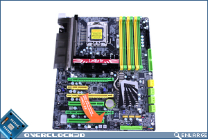
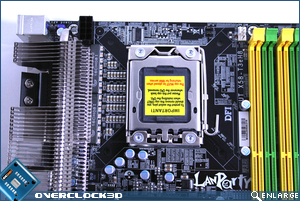
The CPU socket ares is remarkably clear of capacitors and Mosfets. This is down to the Volterra full digital PWM system. Digital PWM allows much cleaner voltages to be supplied to the CPU which in turn can enhance overclocking on the CPU but this undoubtedly adds to the cost of the board. The Motherboard runs on an 8 phase power design which, while appearing low compared to some of it’s competitors ‘claimed’ 16 phase design is more then enough according to DFI.
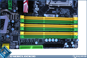
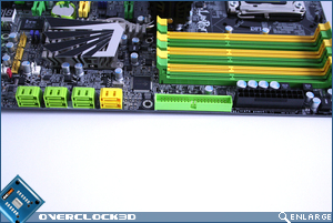
The DDR3 triple channel configuration is the same for all X58 boards thus far, with slots 2+4 for single channel, 2-4-6 for triple channel and all slots can be populated for a maximum supported 24GB of memory.
The board has a plethora of jumper settings, most of which will remain unused for all but the most extreme overclocker. The use of the illuminated on-board Power and Reset switches eradicates the need to operate the CMOS clear jumper as, like its predecessors, if you press both together this will reset the CMOS allowing for a fresh start and returning the motherboard into a bootable state should you become too ambitious with your overclocking.
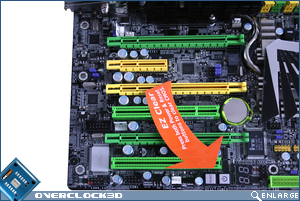
The PCIe layout is very good indeed allowing for Tri SLI use of dual slot cards without any clearance issues. If you do intend on using 3 dual slots cards it is worth considering that, unlike the Gigabyte board we reviewed previously, there will be no remaining PCI/e slots remaining for additional expansion cards. Both Green PCIe slots are 16x until TRI SLI is used and this is where the 8x yellow PCIe slot comes into play. This will throttle the lowest PCIe Green slot back down to 8x with only the uppermost PCIe slot providing the full 16 lanes to the primary GPU.
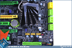
The huge Northbridge heatsink is a break from the previous Ultra editions motherboards in that it is anodised black rather than a brushed aluminium colour. The heatsink does not fit in well with the overall aesthetics of the motherboard not only because of the black heatsink but because of the horrid top plate they have stuck on the sink which sticks out like a sore thumb. To the edge of the board we see that an IDE ports is still available aswell as 8 SATA ports. 6 of the ports are controlled by the ICH10R chip while the remaining 2 yellow ports are controlled by the Jmicron JMB363 chip along with the IDE port. While 8 SATA ports appears plenty, it’s not as many as the Gigabyte UD5 which supply a whopping 10. Whether you need this many will depend on your own circumstances.
The I/O area is sparse compared to some of the other motherboards we have reviewed in the past. No on-board sound, a miserly 6 USB ports, dual Gigabit Lan (with teaming function) and support for PS/2 Keyboard and mouse are all that can be found. Rather than utilise on-board sound, DFI include a separate Bernstein soundcard based on the Realtec ALC 889 codec which, while saving room on the I/O area (which hasn’t been utilised), does take up a PCI backplate. Straddling the I/O area is the largest cooler on the board which takes care of cooling the PWM area. One would think this should be plenty to cool this area, DFI however have other ideas as we shall see.
A very neat little feature of the board is the replaceable BIOS chip should it become corrupted through an incorrect BIOS update procedure. While no replacement BIOS chip is included in the package, taking the chip out and RMA’ing that is much cheaper (and easier) than RMA’ing the whole motherboard.
Removing the top of the Northbridge heatsink we come across an oddity. A solid metal bar nestles between the top and bottom of the heatsink yet there was no thermal paste to aid heat transfer. While this was disappointing at first there is method to DFI’s madness. The metal bar can be removed and the optional Flame Freezer heatsink can be placed here instead of on the I/O backplate area to decrease temps further should this necessity be required.
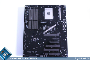
Removing the mid section of the Northbridge and the remainder of the whole heatsink assembly was straightforward enough as the whole heatsink is attached to the motherboard via screws . Using screws instead of push-pin ensures that the best possible contact and mounting pressure is achieved.
Two different pastes were used on the motherboard but all areas had evidence of perfect contact, included the PWM area which is unusual as most manufacturers opt to use thermal tape in this area.
Fitting the flame freezer to the I/O area was a little fiddly and I do question the need for additional cooling here however nobody can doubt the the I/O cooling and indeed the overall cooling of the T3eH8 is awesome and I have no doubts whatsoever that this is perhaps the best cooling solution a motherboard has seen to date.
Well thats the motherboards aesthetics investigated. Time to get this show on the road and take a look at what performance features this board has to offer…


